SDG #169 How to check JLCPCB will manufacture your PCBs correctly
Ordering a batch of boards is cheap; ordering the wrong boards twice is not. This walkthrough covers the verification step most people skip, checking exactly what the fab house sees before money changes hands, using an LED microscope ring light PCB as the working example.
The core idea is that a Gerber set is not the same thing as your PCB layout. Your CAD tool shows you an idealised design; the manufacturer only receives the exported copper, silkscreen, solder mask, paste, drill and outline files. Any export mistake, missing layer, wrong drill file format, unclosed board outline, or a silkscreen that overlaps pads becomes a physical defect on the finished panel. Loading the same zip file into an independent Gerber viewer, rather than trusting the design software’s own render, is the only reliable way to catch that mismatch.
Also covered: reading the fab’s online preview after upload, confirming layer assignment and stack up ordering, checking that plated holes and vias landed where expected, sanity checking the board outline dimensions against what you designed, and reviewing options such as surface finish, mask colour, copper weight and whether panelisation or a specific solder paste stencil is needed for assembly.
For anyone moving from hand built prototypes to ordered boards, the practical takeaway is that a five minute file review is far cheaper than a two week reorder. Building this into your routine before every order, especially when changing CAD packages or export templates, removes most of the common first order disappointments and gives a much clearer picture of what will arrive in the post.
More Electronics Projects
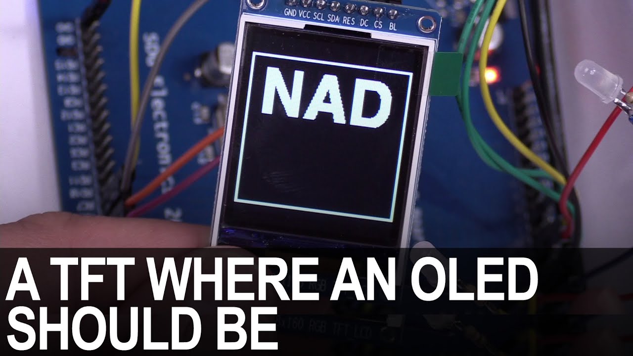
SDG #365 Reverse Engineering NAD D7050 OLED Replacement for IPS TFT
Decoding the NAD D7050's obsolete SSD1355 OLED protocol with a logic analyser, then driving an SSD1351 OLED and ST7735S IPS TFT as replacements.

SDG #360 Zero Crossing Detection and PCBWay 3D Prints
Testing PCBWay nylon PA12 and clear resin wall mounts for a Waveshare 4in ESP32-S3 touch dimmer, plus lower-power zero crossing detection options.

SDG #357 RGB Meteor Shower LEDs Build using ESP32 and WLED
Custom meteor shower Christmas lights built from WS2812 LED PCBs, ESP32 controllers running WLED, acrylic tubes and 3D printed weatherproof caps.