SDG #154 How to do controlled impedance traces on your PCB
Controlled impedance is one of those PCB topics that gets treated as black magic, but it comes down to geometry, dielectric properties and disciplined layout. This walkthrough covers what actually determines the characteristic impedance of a trace: track width, the distance to the reference plane below it, the dielectric constant of the substrate, copper thickness, and in the case of coplanar structures, the gap to the surrounding ground pour.
The two structures most hobbyists will use are microstrip, a signal trace referenced to a solid plane on the layer beneath, and coplanar waveguide with ground (CPWG), where the trace is flanked by ground fill on the same layer and still referenced downwards. CPWG is popular on small boards because the flanking ground lets you use a narrower trace for the same 50 ohm target, but it only behaves as intended if the side grounds are properly stitched to the reference plane with plenty of vias.
The critical practical point is that no calculator output is meaningful without real stackup numbers from the fabricator. Core and prepreg thicknesses, finished copper weight after plating and the Dk of the laminate at your operating frequency all shift the answer, and standard 1.6mm two layer FR4 puts the plane so far away that a 50 ohm microstrip becomes impractically wide. Thinner boards, or routing RF on the outer layers of a four layer stackup with a shallow dielectric, are the sane approach.
Other things that matter in practice: keeping the reference plane continuous under the whole trace, avoiding stubs and sharp discontinuities, managing connector launch geometry, and remembering that below a few hundred MHz on short runs, impedance control often is not worth the layout compromises.
More Electronics Projects
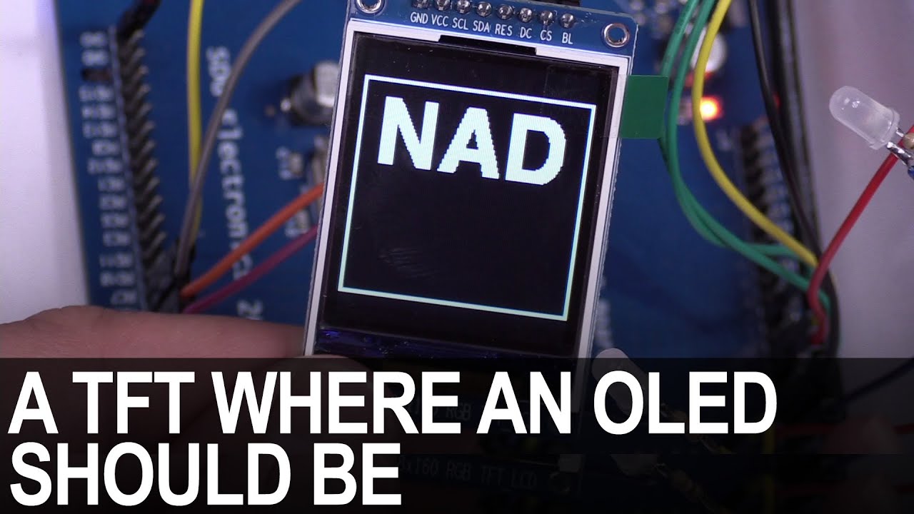
SDG #365 Reverse Engineering NAD D7050 OLED Replacement for IPS TFT
Decoding the NAD D7050's obsolete SSD1355 OLED protocol with a logic analyser, then driving an SSD1351 OLED and ST7735S IPS TFT as replacements.

SDG #360 Zero Crossing Detection and PCBWay 3D Prints
Testing PCBWay nylon PA12 and clear resin wall mounts for a Waveshare 4in ESP32-S3 touch dimmer, plus lower-power zero crossing detection options.

SDG #357 RGB Meteor Shower LEDs Build using ESP32 and WLED
Custom meteor shower Christmas lights built from WS2812 LED PCBs, ESP32 controllers running WLED, acrylic tubes and 3D printed weatherproof caps.