SDG #273 MOSFETs, Gate Drivers and PWM Driver Design
This is a design walkthrough rather than a product review, following the reasoning behind a PWM load driver board from a blank page through to sending files off for fabrication. The starting point is a set of real requirements: voltage rating with headroom, continuous current, and switching frequency, because those three numbers dictate almost everything that follows in part selection.
The practical value here is in the parametric search workflow. Rather than picking a familiar part number out of habit, the selection is narrowed using distributor filters on voltage, current, package and on resistance, then verified against the datasheet. Attention is paid to the parameters that people routinely skim past: RDS(on) quoted at a realistic gate voltage rather than the headline 10 V figure, safe operating area and thermal limits versus the optimistic pulsed current number, and the difference between what a device can survive and what it can do continuously on a modest PCB copper area.
Gate drive gets the most attention, and rightly so. Input capacitance and total gate charge are translated into the peak current a driver has to supply to switch the device in a sensible time, which is what keeps switching losses and device temperature under control. That number then becomes the search criterion for the gate driver itself, alongside supply voltage range, propagation delay and package.
The closing sections cover the schematic, decoupling and gate resistor choices, then layout: keeping the gate loop tight, giving the drain and source paths adequate copper, and specifying board thickness and copper weight when ordering. Useful viewing for anyone whose MOSFET circuits run hotter than the maths suggested they should.
More Electronics Projects
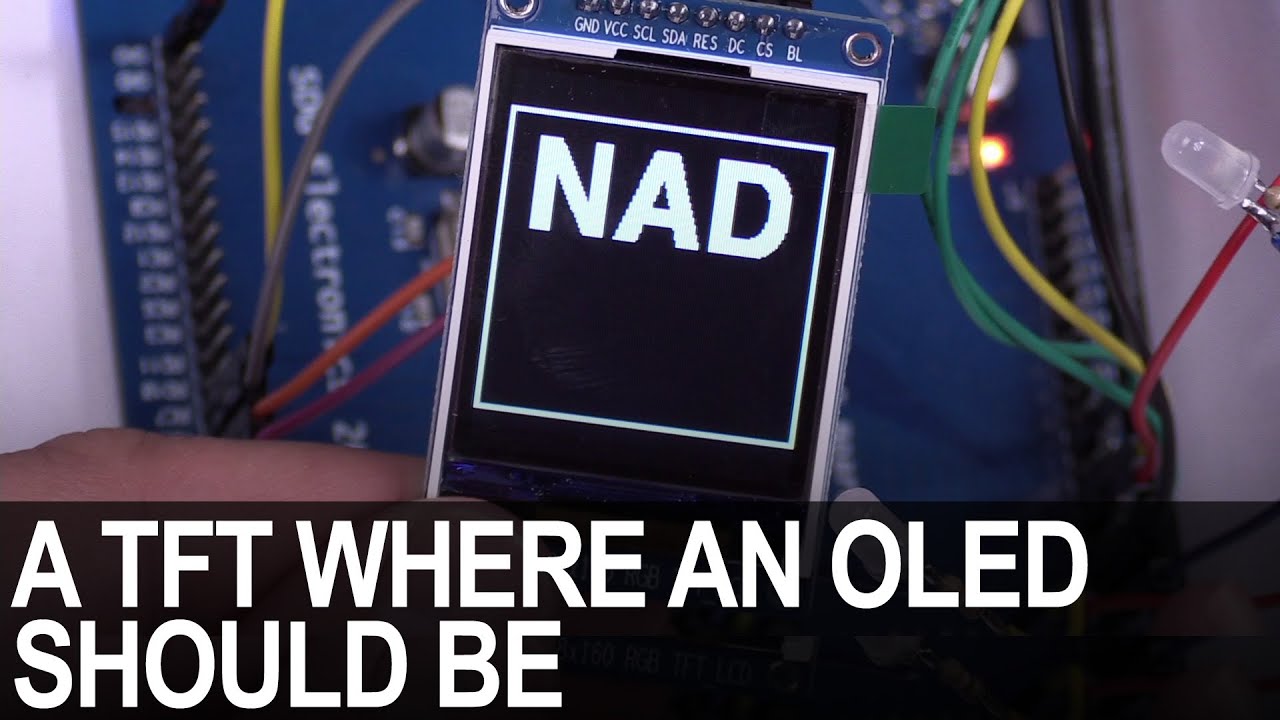
SDG #365 Reverse Engineering NAD D7050 OLED Replacement for IPS TFT
Decoding the NAD D7050's obsolete SSD1355 OLED protocol with a logic analyser, then driving an SSD1351 OLED and ST7735S IPS TFT as replacements.

SDG #360 Zero Crossing Detection and PCBWay 3D Prints
Testing PCBWay nylon PA12 and clear resin wall mounts for a Waveshare 4in ESP32-S3 touch dimmer, plus lower-power zero crossing detection options.

SDG #357 RGB Meteor Shower LEDs Build using ESP32 and WLED
Custom meteor shower Christmas lights built from WS2812 LED PCBs, ESP32 controllers running WLED, acrylic tubes and 3D printed weatherproof caps.