SDG #090 PCB Design Tips and Design Rules
This episode steps away from tool teardowns and looks at the part of hobby electronics where mistakes get expensive: laying out a board that a fab house can actually build correctly the first time. The focus is on design rules, the constraints you set up in your CAD package before routing so the software catches errors rather than the assembly stage doing it for you.
The practical value here is in understanding where those numbers come from. Trace width is driven by current handling and copper weight, clearance by voltage and manufacturing tolerance, and annular ring and drill sizes by what the board house can reliably produce at low cost. Push past a manufacturer’s standard capability and you either pay for advanced spec or receive boards with broken tracks and tented vias that were never meant to be tented. Matching your design rule set to the published capability sheet of the fab you actually intend to use is the single highest value habit a beginner can adopt.
Also covered is the wider layout discipline that a design rule check will never flag: sensible component spacing for hand soldering and rework, keeping test points accessible, silkscreen that survives the printing process at small sizes, and thinking about ground return paths rather than treating a ground pour as automatic good practice.
For anyone who has had a prototype run come back unusable, the lesson is that most respins trace back to constraints that were never entered in the first place. Spend the time on setup before routing and the board largely checks itself.
More Electronics Projects
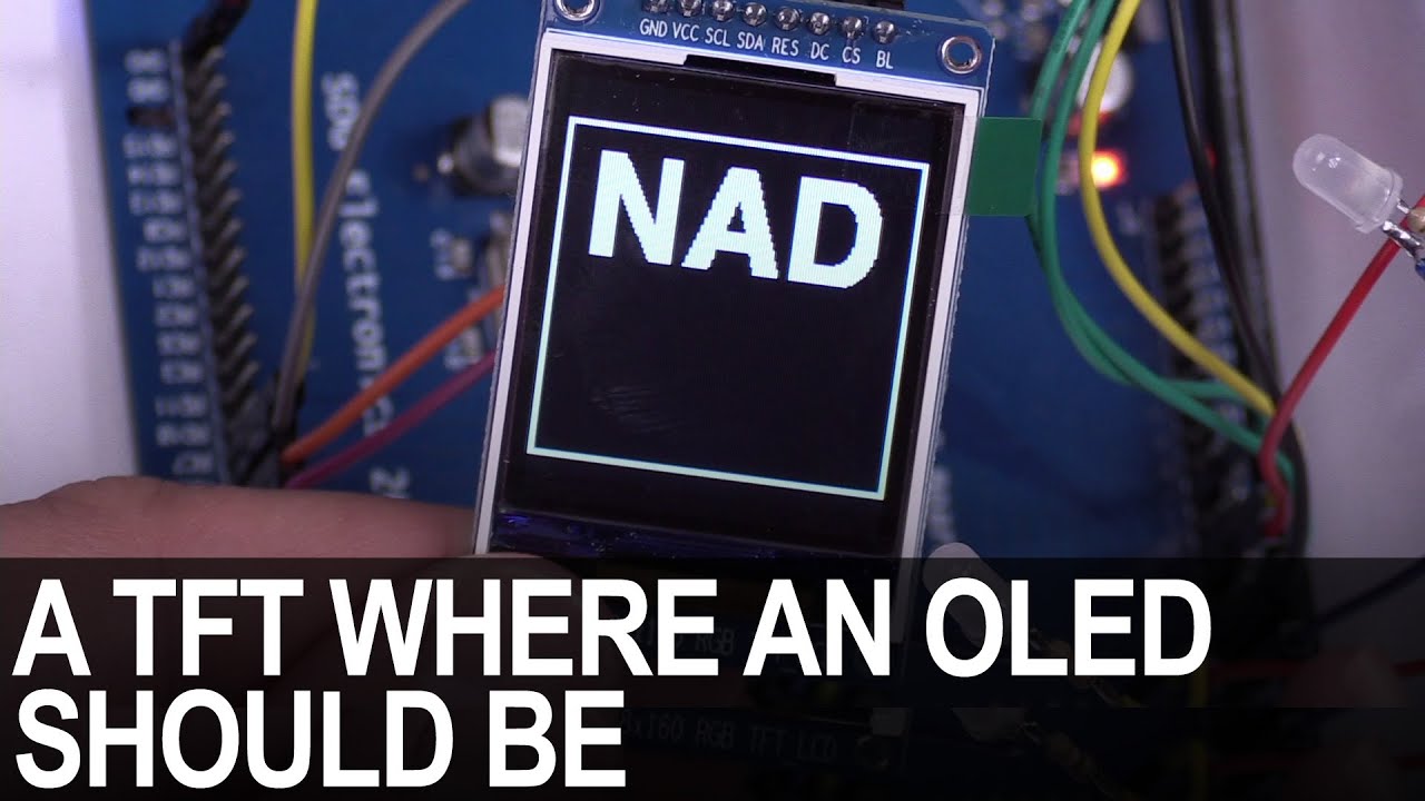
SDG #365 Reverse Engineering NAD D7050 OLED Replacement for IPS TFT
Decoding the NAD D7050's obsolete SSD1355 OLED protocol with a logic analyser, then driving an SSD1351 OLED and ST7735S IPS TFT as replacements.

SDG #360 Zero Crossing Detection and PCBWay 3D Prints
Testing PCBWay nylon PA12 and clear resin wall mounts for a Waveshare 4in ESP32-S3 touch dimmer, plus lower-power zero crossing detection options.

SDG #357 RGB Meteor Shower LEDs Build using ESP32 and WLED
Custom meteor shower Christmas lights built from WS2812 LED PCBs, ESP32 controllers running WLED, acrylic tubes and 3D printed weatherproof caps.