SDG #164 Step-by-step PCB Layout - High Power Microscope LED Light
This instalment continues the high power microscope illuminator project, moving from a finished schematic into a full board layout worked through decision by decision. Rather than presenting a finished file, the process is shown in real time: component placement, board outline definition, net routing, and the compromises that appear once physical constraints collide with the ideal circuit topology.
The interesting engineering content here is thermal. High power LEDs dump most of their input as heat, so the layout treats copper as a heatsink rather than just a conductor. Pad geometry, thermal relief choices, and the use of large pours under the emitters all get attention, along with how the constant current driver stage should be positioned relative to the LEDs to keep sense traces short and switching loops tight. Anyone who has built an LED board that browned its own solder mask will recognise why this matters.
Also useful is the treatment of the board shape itself. A microscope ring light has to clear the objective, sit at a sensible working distance, and mount without fouling the barlow lens, so mechanical dimensions drive the outline before a single track is drawn. That mechanical first approach is a habit worth copying on any project with an enclosure or fixture.
For viewers learning EDA software, the value is watching a competent designer’s workflow rather than a feature tour: how nets are grouped, when to reroute versus nudge a part, and how the design is checked before ordering. It is a practical companion piece to the earlier schematic and constant current driver videos in the series.
More Electronics Projects
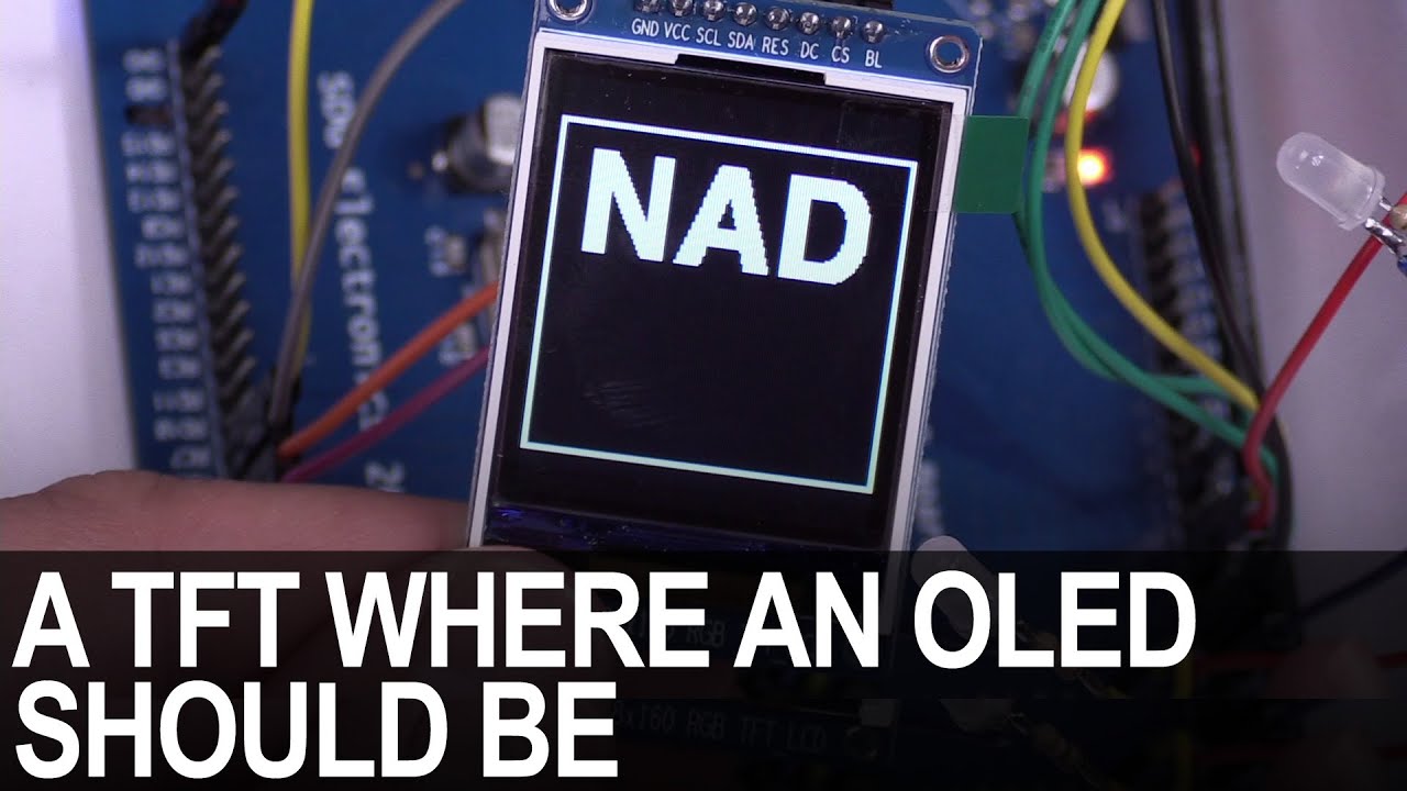
SDG #365 Reverse Engineering NAD D7050 OLED Replacement for IPS TFT
Decoding the NAD D7050's obsolete SSD1355 OLED protocol with a logic analyser, then driving an SSD1351 OLED and ST7735S IPS TFT as replacements.

SDG #360 Zero Crossing Detection and PCBWay 3D Prints
Testing PCBWay nylon PA12 and clear resin wall mounts for a Waveshare 4in ESP32-S3 touch dimmer, plus lower-power zero crossing detection options.

SDG #357 RGB Meteor Shower LEDs Build using ESP32 and WLED
Custom meteor shower Christmas lights built from WS2812 LED PCBs, ESP32 controllers running WLED, acrylic tubes and 3D printed weatherproof caps.