SDG #251 IGBT's, MOSFETs, Trailing Edge Dimmers and Micsig CP210A current probe
This episode sits somewhere between a design post mortem and a probe demonstration. The project under test is a mains trailing edge dimmer, built in two flavours so the switching devices can be compared directly: one board using MOSFETs and another using IGBTs. Along the way there is a genuinely useful refresher on why an IGBT behaves like a hybrid of a BJT and a MOSFET, where the collector saturation voltage penalty bites, and why that penalty matters less as voltage and current climb.
The schematics are walked through before any power is applied, which is the right order for anyone planning to replicate the circuit. Attention then turns to measurement: capturing gate drive and load current on a live mains circuit demands proper isolation, so a differential probe handles voltage while the Micsig CP210A current probe takes care of current without inserting a shunt into the path. That combination, feeding a PicoScope 5000 series, is what makes the switching behaviour visible rather than guessed at.
The waveform comparison is where the real value lies. Turn on and turn off edges, tail current behaviour and the differences in dissipation between the two device families show up clearly, and the maths channel functions in the early access PicoScope 7 build are used to derive instantaneous power from the voltage and current traces. That is the sort of workflow worth borrowing whether or not you ever build a dimmer.
The closing section is honest about what did not work as intended and what would change on a revised board, which makes this more instructive than a straightforward success story. Anyone specifying switching devices for mains loads, or weighing up a clamp style current probe for switching measurements, will find plenty to take away.
More Electronics Projects
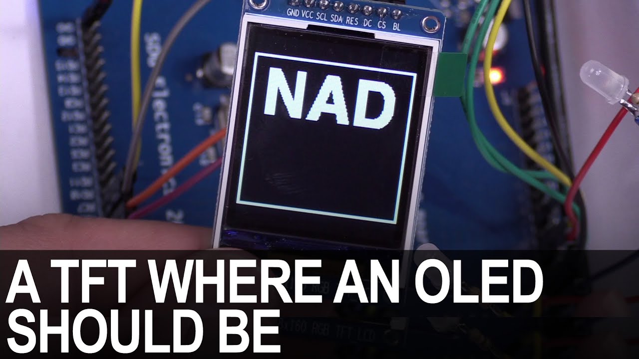
SDG #365 Reverse Engineering NAD D7050 OLED Replacement for IPS TFT
Decoding the NAD D7050's obsolete SSD1355 OLED protocol with a logic analyser, then driving an SSD1351 OLED and ST7735S IPS TFT as replacements.

SDG #360 Zero Crossing Detection and PCBWay 3D Prints
Testing PCBWay nylon PA12 and clear resin wall mounts for a Waveshare 4in ESP32-S3 touch dimmer, plus lower-power zero crossing detection options.

SDG #357 RGB Meteor Shower LEDs Build using ESP32 and WLED
Custom meteor shower Christmas lights built from WS2812 LED PCBs, ESP32 controllers running WLED, acrylic tubes and 3D printed weatherproof caps.